所屬科目:研究所、轉學考(插大)◆電子學
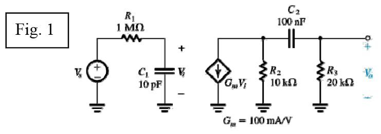
1. (15%) For the circuit shown in Fig. 1 first, evaluate T i(s)=Vi(s)/Vs(s) and the correspondingcutoff (corner) frequency. Second, evaluate T o(s)=Vo(s)/Vi(s) and the corresponding cutofffrequency. Put each of the transfer functions in the standard form and combine them to form theoverall transfer function, T(s)=Ti(s)×To(s). Provide a Bode magnitude plot for ∣T(jw)∣. Whatis the bandwidth between 3-dB cutoff points?
(a) Find the resistances looking into node 1, R1; node 2, R2; node 3, R3; and node 4, R4.
(b) Find the current I1, I2, I3, and I4 in terms of the input current I.
(c) Find the voltages at nodes 1, 2, 3, and 4, that is V1, V2, V3, and V4 in terms of (IR).
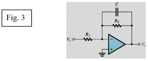
3. (15%) Fig. 3 shows a circuit that performs a low-pass STC function. Such a circuit is known asa first-order low-pass active filt er. Derive the transfer functi on, the dc gain and the 3-dBfrequency. Design the circuit to ob tain an input resistance of 1k Ω, a dc gain of 20dB, and a 3dBfrequency of 4kHz. At what frequency does the magnitude of the transf er function reduce tounity?
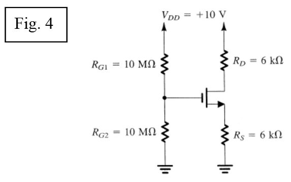
4. (10%) Analyze the circuit shown in Fig. 4 to determine the voltages at all nodes and the currentsthrough all branches. Let V t = 1V and k 'n(W/L) = 1 mA/V 2. Neglect the channel-lengthmodulation effect (i.e., assume λ=0). (10%)
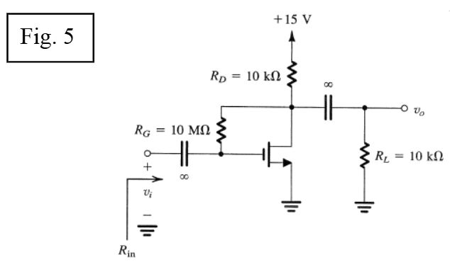
5. (20%) Fig. 5 shows a discrete common-source MOSFET amplifier utilizing the drain-to-gatefeedback biasing arrang ement. The input signal vi is coupled to the gate via a large capacitor,and the output signal at the drain is coupled to the load resistance RL via another large capacitor.We wish to analyze this amplifier circuit to determ ine its small-signal vo ltage gain, its inputresistance, and the largest allowable input signal. The transistor has V t = 1.5 V, k’n(W/L) = 0.25mA/V2, and V A = 50 V. Assume the coupling capacitors to be sufficiently large so as to act asshort circuits at the signal frequencies of interest.
(a) Find the differential gain, the common-mode gain, and the common-mode rejection ratio(in dB) if the output is taken single-endedly and the circuit is perfectly matched.
(b) Repeat (a) when the output is taken differentially.
(c) Repeat (a) when the output is taken differentially but the drain resistances have a 1%mismatch.
7. (10%) Sketch a CMOS logic circuit that realizes the Boolean function \( Y = \overline{A + B \bullet (C+D)} \)
 阿摩線上測驗
登入