 阿摩線上測驗
題組內容
6. Design the circuit of Fig. 4 for an enhancement MOSFET having \( V_t = 2\text{ V} \) and \( k'_n(W/L) = 2\text{ mA/V}^2 \). Let \( V_{DD} = V_{SS} = 10\text{ V} \).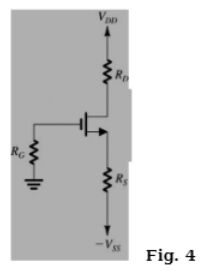
(a) Design for the largest possible “RD” (for a dc bias current of 1 mA and for the largest possible voltage gain consistent with allowing a 2-V peak-to-peak voltage swing at the drain.) (10%)