6. The design of a class AB MOS output stage, as shown in Fig. 6,is being considered, where each transistor has |Vt| = 1 V and μCoxW/L = 300 mA/V2.
What value of gate-to-gate bias voltage “VGG” is required suchthat the incremental output resistance of the equivalent circuitin the quiescent state is 25 Ω? (15%)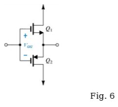
 阿摩線上測驗
登入
阿摩線上測驗
登入